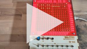
Eris 2206 FPGA Computer
Eris 2206 is a front-panel programmable 8 bit computer with lots of Blinkenlights, implemented on an FPGA. It is not directly based on an existing computer design (contemporary or historic), but it takes inspiration from minicomputers and early microcomputers.
- Video ⟸ Watch the video!
- Repository (Clone) ⟸ Eris 2206 source code. It’s free!
Introduction
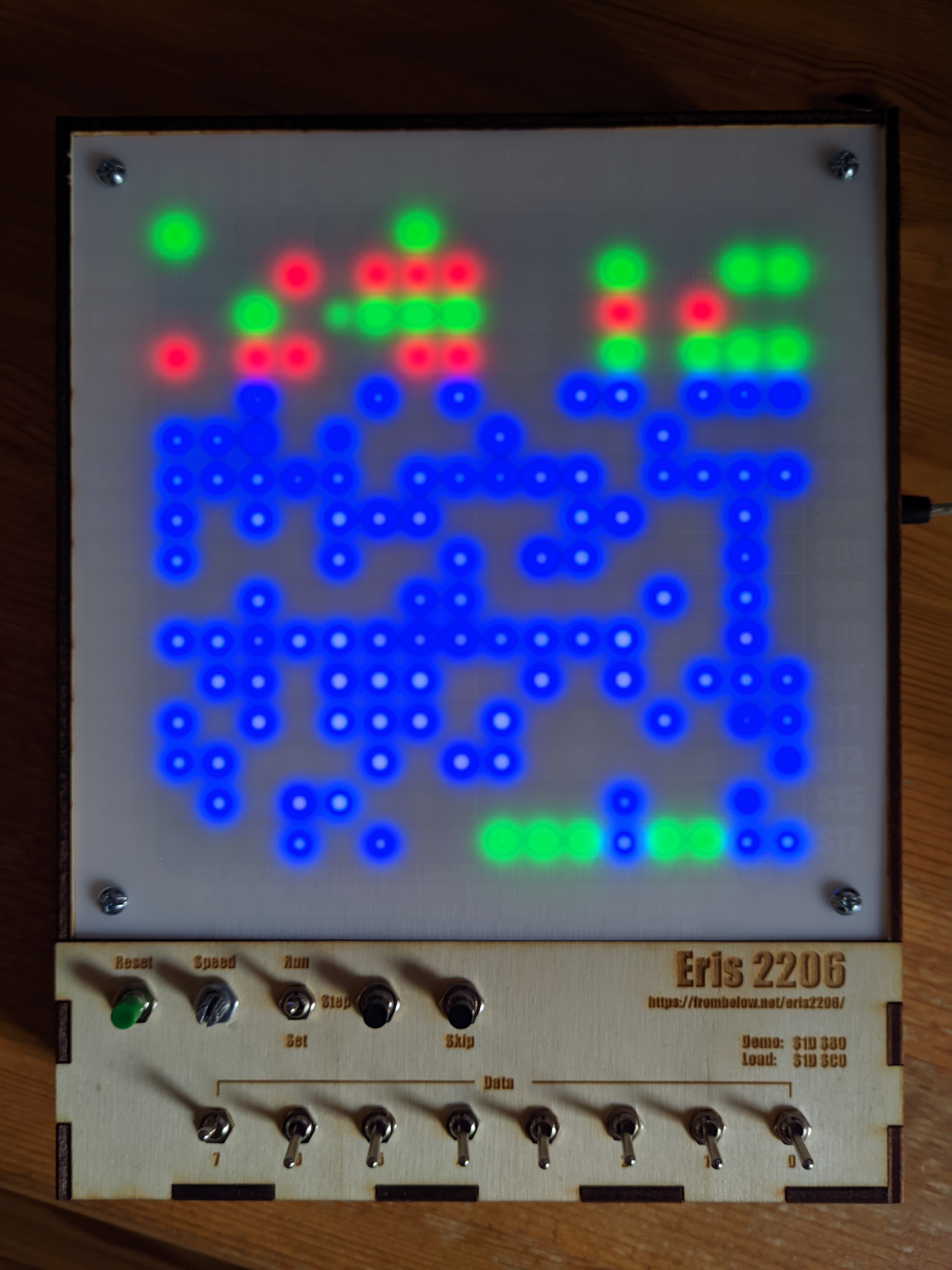
The most prominent feature of Eris 2206 is its 16x16 LED display, which shows the internal state of the CPU and the first 24 memory addresses. The main mode of programming Eris 2206 is by directly writing to its 128 bytes of RAM via front-panel switches. The 125 bytes ROM contain a small bootloader to load programs and data via a serial connection.
Operating Eris 2206
Eris 2206 knows three operation modes: run mode, step mode, and memory set mode. The mode is chosen by a three way switch. In run mode, execution speed is set by the speed dial next to the mode switch, while in step mode the step button triggers execution of the next micro instruction.
Eris 2206 powers on when connected to a USB power supply. On power up in run or step mode, it starts executing the program located at the first ROM address, $80, which computes Fibonacci numbers.
The 16x16 LED matrix shows the internal state of the CPU and the first RAM cells:
| Row | Left Side | Right Side |
|---|---|---|
| 0 | Micro Instruction | Micro Instruction |
| 1 | Address Bus | Data Bus |
| 2 | Accumulator | ALU |
| 3 | Program Counter | Data Pointer |
| 4-15 | RAM | RAM |
Programming
The main mode of programming Eris 2206 is by front panel switches. For this, the mode switch has to be set to memory set mode. Pushing the reset button sets the memory address to the first address, $00. Now the data bus can be set via switches. Pushing the step button writes the current value on the data bus to the current memory address and advances the memory pointer. Pushing the skip button advances the memory pointer without writing to memory. When program and data have been written to memory, execution is started by setting the mode button to step mode and pushing the reset button. Now the program is executed by pushing the step button repeatedly or by switching to run mode.
Alternatively, programs can be uploaded via the serial UART provided
by the USB interface. For this, a minimal first-stage boot loader has
to be programmed and executed via the front panel. This first-stage
boot loader jumps to the second stage serial boot loader at ROM
address $C0. The host program for serial upload is located in
directory src/tools/send_serial.py. It expects hex code input.
Memory
Since we have an 8 bit address bus, a total of 256 memory addresses are available. The lower 128 bytes are RAM. The upper 125 bytes are RAM. The uppermost three bytes provide memory mapped access to I/O and the UART.
| Address | Assignment |
|---|---|
| $FF | UART - Clear/Status |
| $FE | UART - Send/Receive |
| $FD | I/O (0..5: LEDs) |
| $C0-$FC | ROM (Serial boot loader) |
| $80-$BF | ROM (Fibonacci numbers) |
| $00-$7F | RAM |
Assembler
src/tools/eras.pl provides a macro assembler using CPP for macro
processing. The directory also contains a number of example programs.
The CPU knows four addressing modes:
- Implicit
The argument is given implicitly, e.g. INC, which adds one to the accumulator.
- Immediate
The argument is the actual value. This mode is indicated by a “#”. Example: LDA #$5C loads the value $5C into the accumulator.
- Direct
The argument is the memory location of the actual value. Example: LDA $5C loads the value stored at memory address $5C into the accumulator.
- Indirect
The argument is the memory address where the memory address of the actual value is located. This mode is indicated by “()”. Example: If memory address $5C contains value $3B, and memory address $3B contains value $67, LDA ($5C) loads $67 into the accumulator.
| Op. | Imp. | Imm. | Dir. | Ind. | Description |
|---|---|---|---|---|---|
| NOP | $00 | No operation | |||
| LDA | $08 | $02 | $0B | Load accumulator | |
| STA | $12 | $17 | Store accumulator | ||
| JMP | $1D | Jump to address | |||
| JNZ | $21 | Jump if accumulator != 0 | |||
| JZE | $25 | Jump if accumulator == 0 | |||
| ADD | $38 | $29 | $30 | Add value to accumulator | |
| SUB | $4B | $3C | $43 | Subtract value from accumulator | |
| AND | $5E | $4F | $56 | Logical AND of accumulator and value | |
| ORA | $71 | $62 | $69 | Logical OR of accumulator and value | |
| XOR | $84 | $75 | $7C | Logical XOR of accumulator and value | |
| INC | $88 | Increment accumulator | |||
| DEC | $8A | Decrement accumulator | |||
| ROL | $8C | Rotate accumulator 1 bit left | |||
| ROR | $8E | Rotate accumulator 1 bit right | |||
| INV | $90 | Invert accumulator |
Example
We write a program that adds $05 and $06:
start:
	LDA #$05
	ADD #$06
	STA :result
	JMP :start
result:
The assembler generates the following machine code for this:
08 05
38 06
12 08
1D 00
In order to enter the machine code, we set the mode switch to “set”, and push the reset button. Now we enter each byte, followed by pushing “step”. Once we are done, we set the mode switch to step, push reset, and set the mode switch to run. After a number of steps, the result is shown memory address $08.
If we want to add different numbers, we set the mode to set again, push reset, push skip once in order to advance to memory address $01 without overwriting the LDA instruction, set the first new number, push step, push skip in order to advance to memory address $03, set the second new number, and set the mode switch to run.
I/O and UART
The I/O register simply maps the lowest 5 bits to the LEDs on the iCEstick (which are not visible, since the iCEstick is in the case).
The UART utilizes two addresses: One address for sending and receiving data, and a second address for status information and to clear the input buffer.
The byte written to address $FE is send. While the bit is transmitted,
bit 0 of $FF is 1 (tx_busy). In order to receive a byte, the receiver
buffer must be cleared by writing any value to $FF. Once a byte is
received, bit 1 of $FF is 1 (recv_buffer_full). Now the byte can be
read from $FE. In order to receive the next byte, the receive buffer
has to be cleared again. See src/roms/rom_uart.asm for an example.
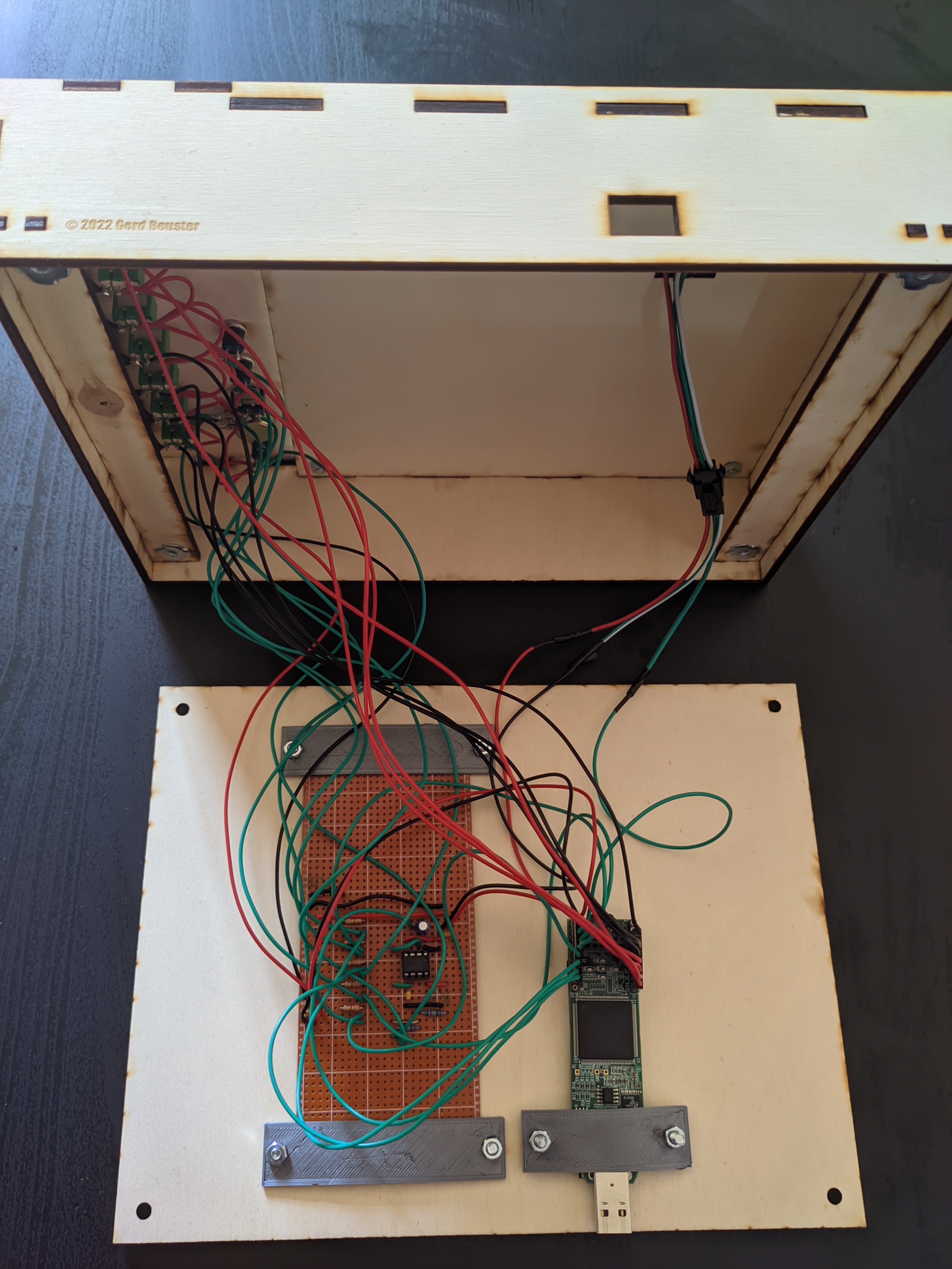
Hardware
Eris2206 is implemented on an iCEstick FPGA Evaluation Kit. It is synthesized using the free tools of project IceStorm.
The GPIO pins of the FPGA connect to the 16x16 (WS2811) matrix display and the buttons/switches. Beside some pull-down resistors, the only additional hardware is an NE555 multivibrator circuit providing the bus clock. The speed dial changes the frequency of the multivibrator.
SOC
See doc/schematic.dia for an overview of the SOC. Besides the CPU core,
the main peripherals are memory (RAM and ROM), the UART, and a system
monitor providing output to a matrix of WS2811 LEDs.
CPU
The following description of the internal works of the CPU should help
you to understand the implementation in src/ecpu.v. It is not
necessary to operate Eris 2206.
An instance of module control_logic orchestras the components of the
CPU. (These control lines are not shown in the schematic.) Microcode
implementations of the opcodes govern the operation of the control
logic. The microcode for the assembler opcodes is defined in and
generated by src/tools/mc_compiler.py.
The CPU has two counters and three registers:
The program counter (PC) points to the next instruction/argument to be processed. The micro instruction pointer (MIP) points to the next micro instruction to be executed. These counters can be set or incremented.
The three registers are the data pointer (DP), the accumulator, and the output of the arithmetic-logic unit (ALU).
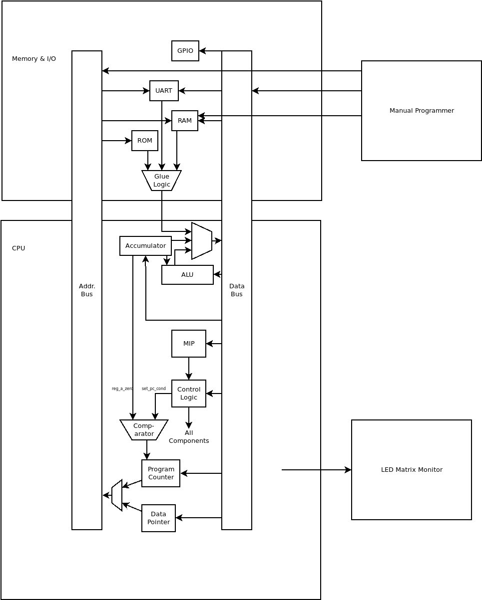
The accumulator is the only register visible to the user. It reads from and writes to external memory (and memory mapped I/O modules) via the data bus. In addition to read and write operations, the accumulator can be incremented, decremented, rotated (left and right), and inverted.
The ALU operates on the current value of the accumulator and the current value on the data base, and writes back to the data bus.
Like the PC, the DP does not write to the data bus, but to the address bus. It is used to dereference addresses in direct and indirect addressing mode.
A zero flag, i.e. a wire indicating whether the register value is zero, is available for the accumulator. This flag is used by the comparator in order to implement the conditional jump on (not) zero instructions.
A little bit of glue logic multiplexes the data and address line: Only the active component may write to the buses.
Micro instructions consist of 15 bits:
| Bit | Operation |
|---|---|
| 0 | Write data bus to PC |
| 1 | Write data bus to PC if zero flag 1 |
| 2 | Write data bus to PC if zero flag 1 |
| 3 | Increment PC |
| 4 | Write data bus to DP |
| 5 | Write DP to address bus (write PC to address bus if bit 5 = 0) |
| 6 | Set memory address on address bus to value on data bus |
| 7 | Write accumulator to data bus |
| 8-10 | Set/increment/decrement/rotate/invert accumulator |
| 11 | Set MIP to value on data bus (increment MIP if bit 11 = 0) |
| 12-14 | Add/subtract/and/or/xor data bus to accumulator and write to data bus |
The implementation of the opcodes as micro instructions is given in
src/tools/mc_compiler.py. mc_compiler.py compiles a ROM file of
the micro instruction implementations of all opcodes. The machine code
(= byte value) of an opcodes is the entry points for the microcode of
its implementation in this ROM file. Therefore in order to decode an
opcode, its byte code is read from the data bus and written into the
MIP.
On negative edges of the clock, the next micro instruction is set, i.e. components are turned on/off according to the micro instruction. The components operate on positive clock edges.
There is a separate clock port for the UART, because the UART must be run at 12 MHz for timing reasons, while the rest of the SOC may run at a lower speed.
LED Matrix Monitor
A 16x16 LED matrix provides a monitor view into the internals of the
SOC. The LEDs are driven by WS2811 controllers. The control logic is
implemented in src/ws2811.v. On each iteration of the internal (12
MHz) clock of the FPGA, one 8 bit element of the monitor is updated,
i.e. it takes 32 cycles to update the complete LED matrix. The WS2811
driver allows to set the three color channels of each LED on or
off. The intensity is fixed for all LEDs and color channels.
Case and Electronics
Case
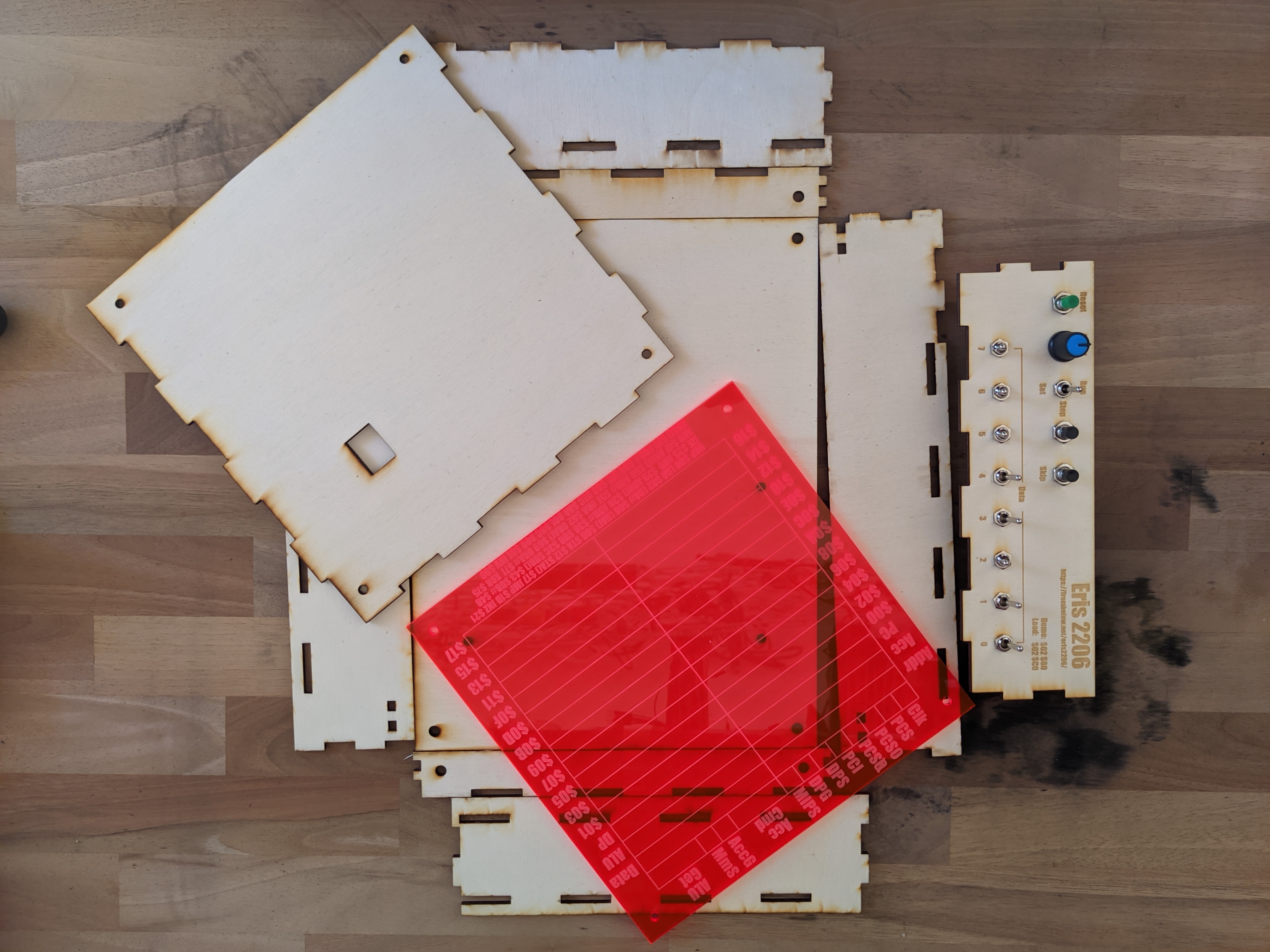
The case has been designed in OpenSCAD. The main design file is
case/case.scad. Most elements of the case can be cut from 6 mm ply
wood with a laser cutter. Running make in directory case generates
cutouts for a laser cutter in case/dst/svg/. Three elements are not
only cut, but also engraved. Engravings have been added manually using
Inkscape. These files for laser cutting are located in
case/dst/labeled. Note that for
case/dst/labeled/top_plate/acryl_top_plate.svg not 6 mm plywood, but
an acryl plate should be cutted.
The holders for the iCEstick and the circuit board are 3D printed. After running make in directory case/, the 3D print files are located in directory case/dst/stl.
The case is partly glued and partly held together by M4 screws. Most M4 screws have nuts as counterparts, except the four screws in the bottom. These are held by claw nuts.
Electronics
The NE555 multivibrator is housed on a small circuit board, together with a bunch of pull-down resistors for the switches. A Fritzing design file is given in board/circuit.fzz. See src/ecpu.pcf for how to connect the hardware components to the GPIO I/O pins.
License
See case/lasercut/LICENSE for author, copyright, and licensing information of the lasercut library.
Everything else:
Copyright © 2022 Gerd Beuster gerd@frombelow.net
This project is free soft- and hardware: you can redistribute it and/or modify it under the terms of the GNU General Public License as published by the Free Software Foundation, either version 3 of the License, or (at your option) any later version.
This project is distributed in the hope that it will be useful, but WITHOUT ANY WARRANTY; without even the implied warranty of MERCHANTABILITY or FITNESS FOR A PARTICULAR PURPOSE. See the GNU General Public License for more details.
You should have received a copy of the GNU General Public License along with this project. If not, see http://www.gnu.org/licenses/.